• A
  • A
  • A
  • АБВ
  • АБВ
  • АБВ
  • A
  • A
  • A
  • A
  • A
Обычная версия сайта
  • RU
  • EN
  • HSE University
  • Publications
  • Book chapter
  • Определение электрофизических параметров высокоомных полупроводников при подсветке образца красным излучением регулируемой интенсивности
  • RU
  • EN
Расширенный поиск
Высшая школа экономики
Национальный исследовательский университет
Priority areas
  • business informatics
  • economics
  • engineering science
  • humanitarian
  • IT and mathematics
  • law
  • management
  • mathematics
  • sociology
  • state and public administration
by year
  • 2028
  • 2027
  • 2026
  • 2025
  • 2024
  • 2023
  • 2022
  • 2021
  • 2020
  • 2019
  • 2018
  • 2017
  • 2016
  • 2015
  • 2014
  • 2013
  • 2012
  • 2011
  • 2010
  • 2009
  • 2008
  • 2007
  • 2006
  • 2005
  • 2004
  • 2003
  • 2002
  • 2001
  • 2000
  • 1999
  • 1998
  • 1997
  • 1996
  • 1995
  • 1994
  • 1993
  • 1992
  • 1991
  • 1990
  • 1989
  • 1988
  • 1987
  • 1986
  • 1985
  • 1984
  • 1983
  • 1982
  • 1981
  • 1980
  • 1979
  • 1978
  • 1977
  • 1976
  • 1975
  • 1974
  • 1973
  • 1972
  • 1971
  • 1970
  • 1969
  • 1968
  • 1967
  • 1966
  • 1965
  • 1964
  • 1963
  • 1958
  • More
Subject
News
September 11, 2026
How to Assess Students Knowledge in the Age of AI
A researcher at HSE University has proposed a flowchart to help lecturers decide how to assess students who use artificial intelligence. It shows where the use of AI should be restricted and where it can be incorporated into the learning process. The article has been published in IT Professional.
September 9, 2026
‘Balkan Hospitality Opens Doors: Studying Dialects on the Verge of Extinction
You cannot study spoken dialects from books. Instead, you need to go to a village, seek out its elders, and earn the trust of local residents before you can record hours of spontaneous stories. This is how Natalia Muravleva, Associate Professor at the Faculty of Humanities, conducts her research. Her internship in Serbia continued her long-standing study of dialects spoken by Macedonian settlers. In this interview, she discusses how diaspora cultural centres help researchers reach informants, why native speakers need to be interviewed only in their own language (otherwise, as she puts it, they may 'break'), and how a single field season helped her finalise her monograph. She also shares warm memories of autumn in Belgrade and of colleagues with whom grammar can be discussed in three languages at once.
September 9, 2026
Scientists Train Neural Network to Generate Process Plans from 3D Models
Researchers at the HSE FCS AI and Digital Science Institute have developed CAD2TechSpec, a framework that converts 3D models of mechanical parts into machining process plans—step-by-step instructions for machine tools. The solution aims to reduce the time required for the design and preparation of technical process documentation in mechanical engineering, aircraft manufacturing, and other high-tech industries. The study findings have been published in PeerJ Computer Science.


Have you spotted a typo?
Highlight it, click Ctrl+Enter and send us a message. Thank you for your help!

Publications
  • Books
  • Articles
  • Chapters of books
  • Working papers
  • Report a publication
  • Research at HSE

?

Определение электрофизических параметров высокоомных полупроводников при подсветке образца красным излучением регулируемой интенсивности

Гл. 64. С. 441–444.
Lysenko A. P., Golubiatnikov V. A., Grigoryev F. I., Strogankova N. I., Белов А. Г.

It is known that illumination of the sample vysokomnogo semiconductor material significantly changes its electrical properties. It is shown that the contact regions of the sample illumination with monochromatic radiation intensity adjustable with a photon energy greater than the width of the forbidden zone of the test material, reduces the resistance of the sample, in some cases by several orders of magnitude. Provides a method for the separate determination of the resistance of the sample and contacts to it, which has been tested on a sample of semi-insulating n-GaAs. It is shown that the resistance of the sample volume and the total resistance of the contacts are close to each other and equal to about 5  108 ohms.

Language: Russian
Full text
Keywords: фотоэмиссияомический контактвысокоомный полупроводникphotoemissionhigh-resistivity semiconductoran ohmic contact

In book

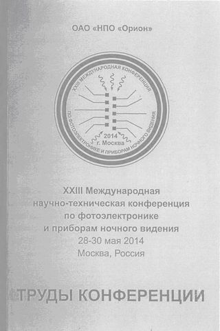
XXIII Международная научно-техническая конференция по фотоэлектронике и приборам ночного видения 28-30 мая 2014, Москва, Россия
М.: ОАО "НПО "Орион", 2014.
Similar publications
Local and Global Directionality Patterns of Electron Photoemission from Plasmonic Nanoparticles
Ikhsanov R., Protsenko I., Smetanin I. et al., Journal of Physical Chemistry C 2023 Vol. 127 No. 50 P. 24223–24232
Concepts of local and global photoemission directivity patterns are introduced for plasmonic nanoparticles of arbitrary shape, and the relationship between them is established. Formulas for the local photoemission directionality pattern for surface and volume photoemission mechanisms are obtained for a given field distribution in plasmonic modes inside nanoparticles of arbitrary shape. As an illustration of the theory, the local and ...
Added: September 5, 2023
Photo-electron emission directly in superfluid helium
Zavyalov V., Pyurbeeva E. B., Khaldeev S., , in: 28th International Conference on Low Temperature Physics.: M.: Faculty of Physics, MSU, 2017. Ch. 012085 P. 1–5.
Despite the fact that electron transport in condensed helium has been studied for over half a century [1], observations of new intriguing effects still appear [2]. Alas, the traditional methods of injecting electrons into condensed helium (radioactive-sources, electrical discharge or field emission) lead to generation of helium ions, recombination of which is accompanied by emergence of a large number ...
Added: October 23, 2019
Photo-electron emission directly in superfluid helium
Zavyalov V., Pyurbeeva E. B., Khaldeev S., Journal of Physics: Conference Series 2018 Vol. 969 Article 012085
Despite the fact that electron transport in condensed helium has been studied for over half a century [1], observations of new intriguing effects still appear [2]. Alas, the traditional methods of injecting electrons into condensed helium (radioactive-sources, electrical discharge or field emission) lead to generation of helium ions, recombination of which is accompanied by emergence of a large number ...
Added: November 10, 2018
ОСОБЕННОСТИ СТАЦИОНАРНОЙ ФОТОПРОВОДИМОСТИ ВЫСОКООМНЫХ ПОЛУПРОВОДНИКОВ ПРИ ЛОКАЛЬНОМ ОСВЕЩЕНИИ
Lysenko A. P., Белов А. Г., Каневский В. Е. et al., Известия высших учебных заведений. Физика 2017 Т. 60 № 12 С. 142–149
The phenomenon of photoconductivity has long been well studied. However, in the overwhelming majority of studies, the photoconductivity of semiconductors was studied by illuminating the entire surface of the samples. In this paper we investigated the effect of local illumination, which ensures a high level of injection of free charge carriers on the conductivity of ...
Added: December 25, 2017
Method of separate determination of high-ohmic sample resistance and contact resistance
Golubiatnikov V. A., Grigoryev F. I., Lysenko A. P. et al., Modern Electronic Materials 2015 Vol. 1 No. 3 P. 93–96
A method of separate determination of two-pole sample volume resistance and contact resistance is suggested. The method is applicable to high-ohmic semiconductor samples: semi-insulating gallium arsenide, detector cadmium-zinc telluride (CZT), etc. The method is based on near-contact region illumination by monochromatic radiation of variable intensity from light emitting diodes with quantum energies exceeding the band ...
Added: May 11, 2016
Use of Contact Illumination for HighResistance Semiconductor Conductivity Measurements
Lysenko A. P., Grigoryev F. I., Strogankova N. I. et al., Instruments and Experimental Techniques 2014 Vol. 57 No. 3 P. 326–329
Abstract—It is shown that illumination of ohmic contacts to highresistance cadmium telluride and gallium arsenide samples affects not only the transient resistance of the contact, but the bulk conductivity of samples by increasing the concentration of free charge carriers. The model explaining the increase in the volume con ductivity of the sample under the illumination ...
Added: May 19, 2014
Способ раздельного определения сопротивлений образца высокоомного полупроводника и контактов к образцу
Lysenko A. P., Grigoryev F. I., Golubiatnikov V. A. et al., Известия высших учебных заведений. Материалы электронной техники 2013 № 4 С. 63–66
The method of separate determination of two-pole sample volume resistance and contact resistance is suggested. The method described is applicable to high-ohmic semiconductor samples: semiinsulating gallium arsenide, detector cadmium-zinc telluride (CZT), etc. The method is based on near-contact region illumination by monochromatic radiation of variable intensity from light emitting diodes with quantum energy exceeding band ...
Added: January 29, 2014
Снижение переходного сопротивления омических контактов к высокоомным полупроводникам с помощью оптического излучения
Lysenko A. P., Golubiatnikov V. A., Grigoryev F. I. et al., Заводская лаборатория. Диагностика материалов 2014 Т. 80 № 1 С. 35–38
The attempt is made to decrease transition resistance of ohmic contacts to high-ohmic semiconductors (such as cadmium telluride and semi-insulating gallium arsenide) due to extra free carrier concentration creating in near-contact region by optical stimulation. Various tested construction variants of such contacts are presented in this paper. The illumination is shown to be useful for ...
Added: January 29, 2014
Применение подсветки контактов для измерений проводимости высокоомных полупроводников
Lysenko A. P., Golubiatnikov V. A., Grigoryev F. I. et al., Приборы и техника эксперимента 2014 № 3 С. 93–96
The influence of light illumination of ohmic contacts to high-ohmic gallium arsenide and cadmium telluride samples is investigated. It is revealed, that near-contact –area illumination influences not only upon transition resistance, but also upon volume conductivity of the samples due to increasing of free carrier concentration. The new method of separate determination of ohmic contact ...
Added: January 14, 2014
Фотоэмиссия свободных носителей заряда в высокоомный полупроводник при освещении омических контактов
Lysenko A. P., Grigoryev F. I., Strogankova N. I. et al., В кн.: Вакуумная наука и техника: Материалы ХХ юбилейной научно-технической конференции.: М.: МИЭМ НИУ ВШЭ, 2013. С. 220–222.
The photoemission of free charge carriers into high-ohmic semiconductor created by light illumination of near-contact-area of ohmic contacts to cadmium telluride sample was investigated. It was revealed, that near-contact-area light illumination influences both on contact transition resistance and on volume conductivity of the crystal due to increasing of main charge carrier concentration. The method of ...
Added: October 11, 2013
  • About
  • About
  • Key Figures & Facts
  • Sustainability at HSE University
  • Faculties & Departments
  • International Partnerships
  • Faculty & Staff
  • HSE Buildings
  • HSE University for Persons with Disabilities
  • Public Enquiries
  • Studies
  • Admissions
  • Programme Catalogue
  • Undergraduate
  • Graduate
  • Exchange Programmes
  • Summer University
  • Summer Schools
  • Semester in Moscow
  • Business Internship
  • Research
  • International Laboratories
  • Research Centres
  • Research Projects
  • Monitoring Studies
  • Conferences & Seminars
  • Academic Jobs
  • Yasin (April) International Academic Conference on Economic and Social Development
  • Media & Resources
  • Publications by staff
  • HSE Journals
  • Publishing House
  • iq.hse.ru: commentary by HSE experts
  • Library
  • Economic & Social Data Archive
  • Video
  • HSE Repository of Socio-Economic Information
  • HSE1993–2026
  • Contacts
  • Copyright
  • Privacy Policy
  • Site Map
Edit